Reverse Engineering a 1.5 inch Photoframe
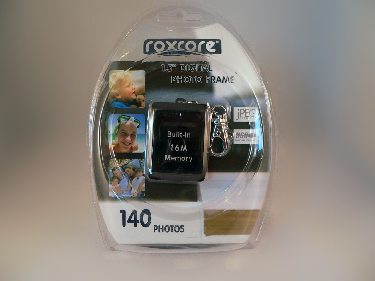
Whilst browsing around a local electronics store I noticed they were selling little key-ring photo frames. These little devices had a 1.5 inch 128×128 colour TFT as well as USB, batteries and 16 Mbytes of storage for around 140 pictures. Best of all they were very cheap, so I purchased a few to see if they could be re-purposed into something useful. Looking on ebay it seems these devices are common-place and it wouldn’t surprise me if most are internally identical. Here is the box for one of the frames I bought:
Out of the three I bought two had LCDs marked FTM144D01N and the other had the marking LC12802.2, however both models looked functionally identical. The issue I found was that there was no available information on the display via Google, the only reference I found was that the FTM144D01N was based on the ILI9163 LCD driver IC from ILITEK.
Since I had more that one, I decided to leave one photo frame intact and remove the screen from the other. This would allow me to analyse the working frame whilst attempting to control the other on the breadboard.
Removing the LCD
To remove the LCD from the photo frame you need some de-soldering braid and a soldering iron with a wide flat tip:
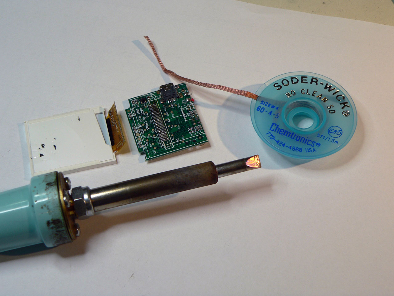
Use a pair of side cutters to remove the Li-Po battery. Make sure you insulate the positive wire once cut so you don’t short the battery. The battery is a 3.7V Li-ion 120mAh cell which is very useful for other projects.
Next place the circuit board in a vice and use the wick to remove the excess solder. Simply heat the soldering iron to about 340C and then place the braid over the connector (partly on the board and partly on the ribbon) then apply the flat soldering tip for a short time to remove the solder.
Once that’s done you hold the LCD in one hand and run the soldering iron across the ribbon whilst gently twisting the LCD free from the circuit. The ribbon should come away easily.
Reverse engineering the connections
The first step to reverse engineering the LCD connections is to simply look at the connector itself. As can be seen in the following picture the ribbon has 27 connections of which many are simply not connected. I’ve marked the unused connections in red:
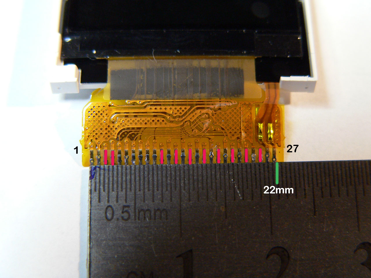
The ruler placed under the ribbon shows that the connector is 22mm approximately. This means that the connector pitch is 22/27 = 0.81; this gives us a connector pitch of 0.8mm (which is pretty typical for a display).
From looking at datasheets for other similar ILI9163 based displays it can be seen that the LCDs are typically 8 or 16 bit parallel interfaces and have 5 control lines: RESET, WR, RD, RS and CS. In addition there are 2 power lines (Vdd and Gnd) and 2 power lines (Anode and Cathode) for the display backlight.
Using a multimeter on the working photo frames showed that pins 1 and 2 are Vdd and Gnd and that pin 26 was the backlight Cathode (positive) and 27 was the backlight Anode (negative).
From the picture above you can also see that there are 8 pins which are all separated by unconnected pins, they also all go to the same group of tracks into the LCD. From that you can easily infer that pins 10, 12, 14, 16, 18, 20, 22 and 24 are the DB0:7 data-bus. This means the LCD is a 8-bit parallel interface. This leaves 5 pins unaccounted for which (thankfully) matches with the expected number of control pins.
The photo frame had a small reset button on the back so identifying the RESET line was as simple as pressing the reset switch and seeing which line dropped using an oscilloscope; this was pin 9.
Finding the rest of the control pins was a little more difficult, using just trial and error would take a long time. Since the ILI9163 data-sheet had some signalling diagrams I decided to compare the pins using a dual-channel oscilloscope to see if they could be identified. Pin 7 was at a constant 3.3Vs in the working photo frame so that was most likely the RD pin since that is the read/write selection (and the photo-frame only needs to write to the display).
The data-sheet information showed that during operation the WR and CS lines would follow each other closely with the CS pulse occurring inside each WR pulse. Testing the various pins combinations showed that this type of pulsing was present on pins 5 and 8 as shown by the following DSO trace:
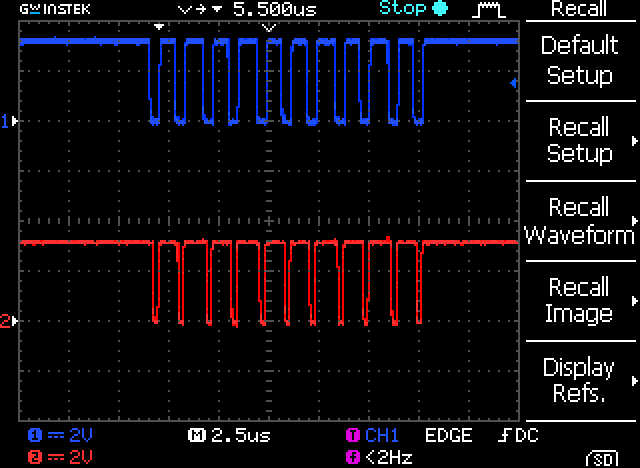
This means that pin 5 is likely to be the WR line and pin 8 is the CS (chip select). This leaves only one spare pin which must be the RS line.
Therefore the pin out for the ribbon connector is as follows:
- Vdd (3.3V)
- Gnd
- NC
- NC
- WR
- RS
- RD
- CS
- RESET
- DB0
- NC
- DB1
- NC
- DB2
- NC
- DB3
- NC
- DB4
- NC
- DB5
- NC
- DB6
- NC
- DB7
- NC
- Back-light cathode (+)
- Back-light anode (-)
Tracing the back-light cathode on the working photo frame also showed that a 4R7 resistor (4.7 ohms) was used to drop the 3.3V supply to the back-light.
Breadboard Adaptor
In order to test out the display it was necessary to connect it to a breadboard. I designed a simple PCB which converts the 0.8mm pitch connections to a standard 2.54mm pin header suitable for connection directly to a breadboard:
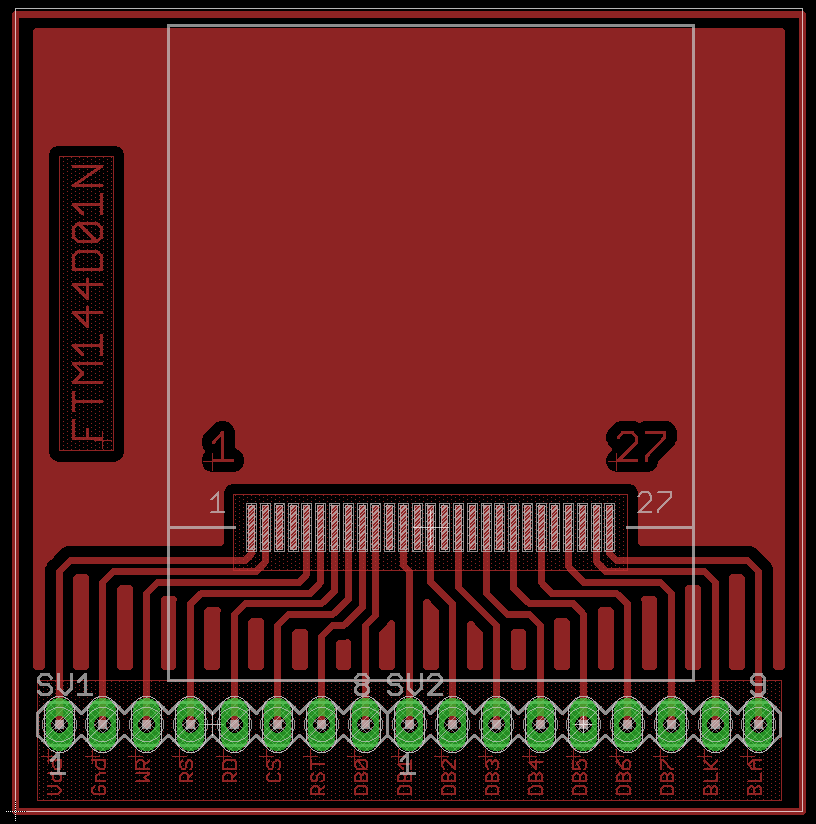
As can be seen in the image, only the required connections are routed to the breadboard to save space. You can also buy 0.8mm pitch adaptor boards from a variety of sources if you don’t want to make your own PCB. The Eagle CAD 6 files for the PCB shown above are available at the end of the article.
To solder the ribbon to the board I used a small piece of sticky-tape to hold the connector in place and then simply applied solder to the connections. Any solder bridges can be quickly removed using some de-soldering braid if required. Note that it’s a good idea to use a flux pen to apply flux to both the PCB and the ribbon before soldering; it helps the solder flow cleaner across the two. Then a standard male single-row 2.54mm pin header was soldered to the PCB to connect to the breadboard.
So that I could test the LCD I designed a simple circuit using an ATmega16u2 micro-controller running at 3.3Vs connected to the display. The choice of processor was only based on what I had to hand, the LCD will work with any common micro-controller. Note that the LCD is designed to work at 3.3Vs; if you want to use a 5V micro-controller you will need to use a couple of 74HC4050N ICs or similar to connect the 3.3V display to the 5V micro-controller.
The test circuit is shown in the following schematic diagram:
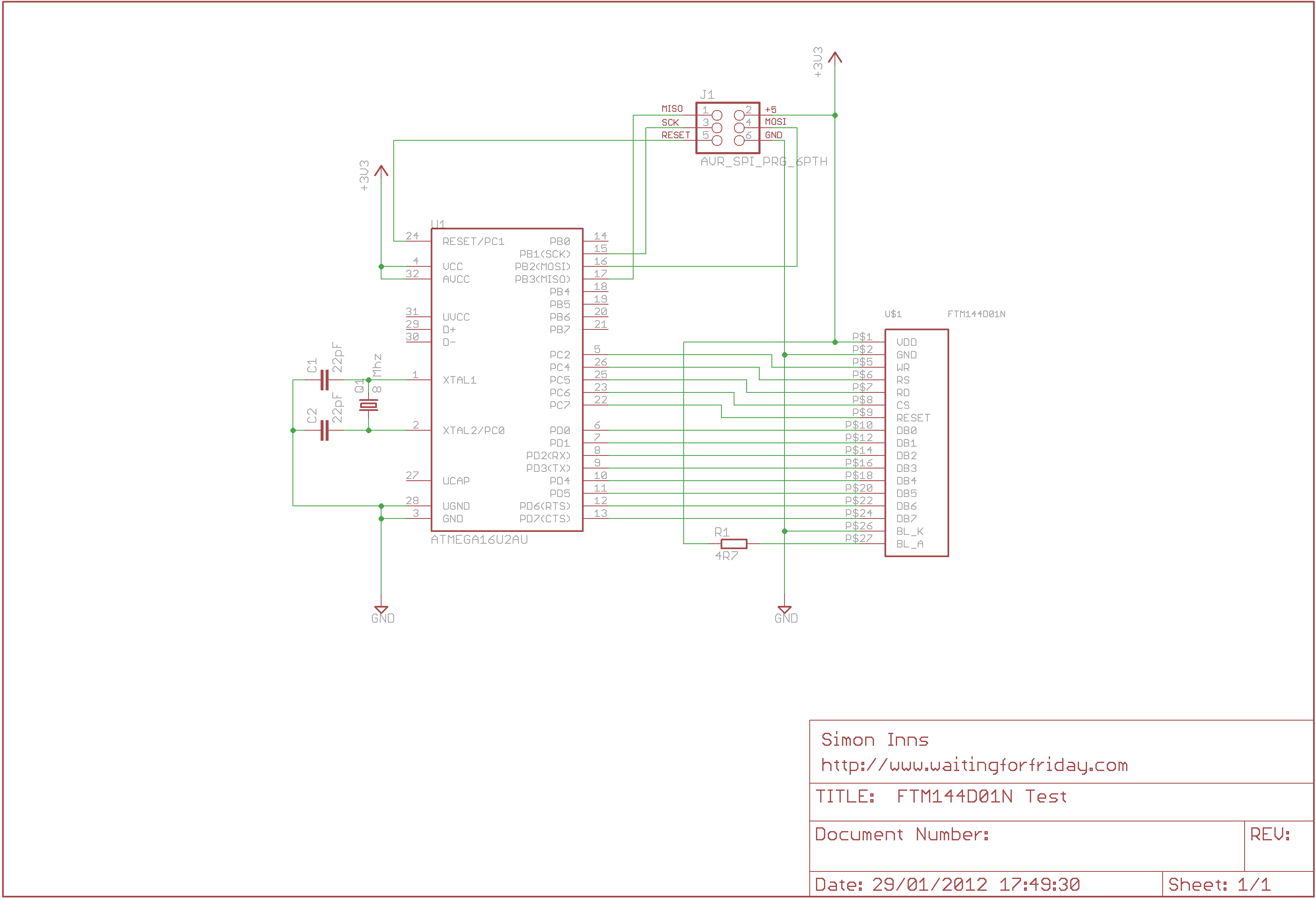
Note that the schematic does not show the 100nF decoupling capacitors. You will need to place some around the power pins for both the micro-controller and the LCD.
ILI9163 driver library
In order to test the LCD I first used some sample ILI9163 code which I found on the web. This was enough to prove it was working but the test code was very poorly written and didn’t provide very much functionality. To use the display in my projects I wrote a better library which provides line drawing (using Bresenham’s algorithms), rectangles, filled rectangles, circles and a 5×8 font for printing strings to the display. The library also provides some simple colour mapping functions to make it easy to select a colour. In addition the LCD initialisation allows you to select from 4 orientations of the LCD so you are free to mount the display any way up you like and then flip the output in software.
Here is a screen shot of the test application in action, at the bottom of the display is a simple bat and ball animation to test the update speed of the display (which is very quick for such a cheap TFT LCD):
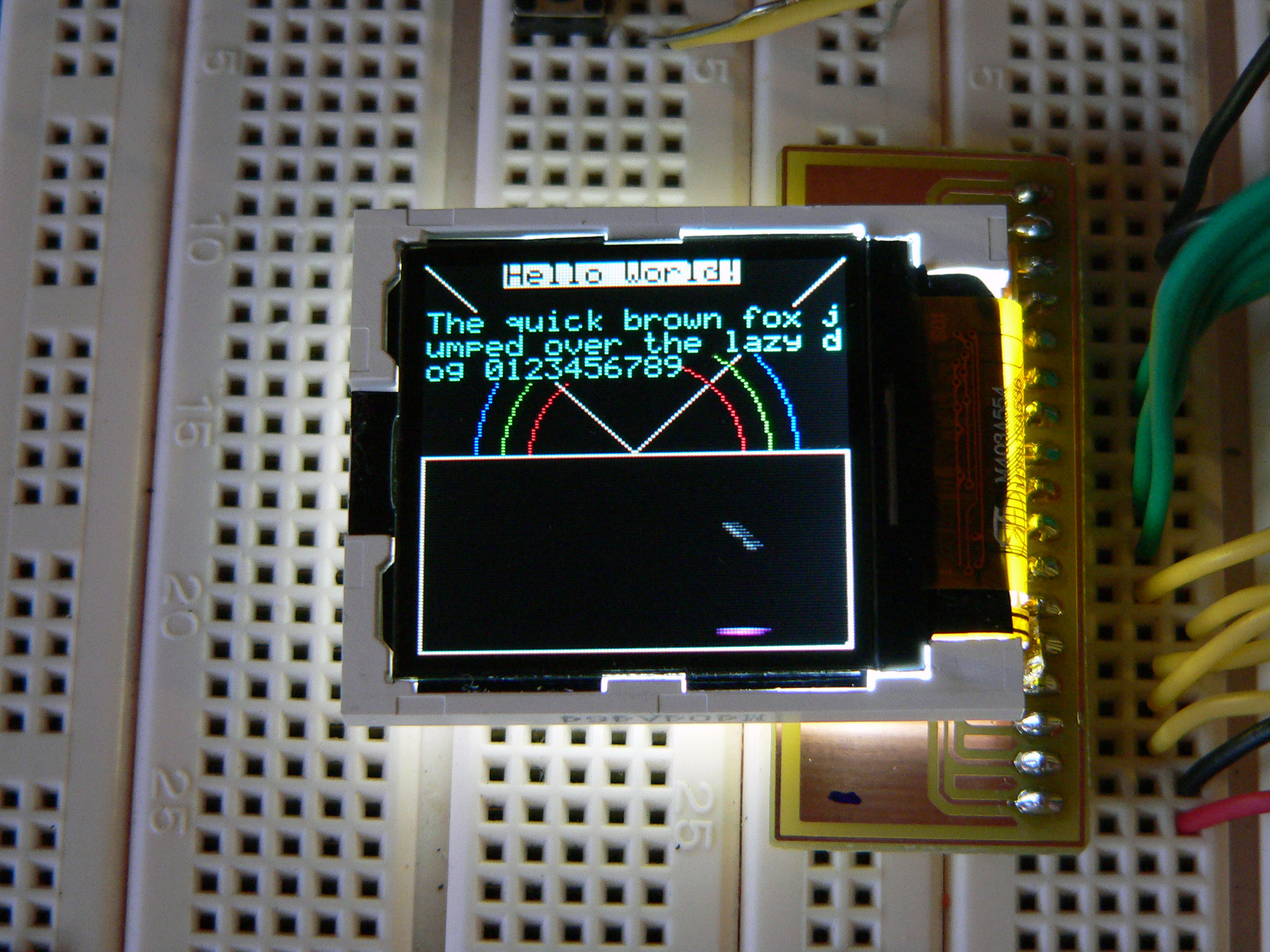
The library is quite simple at the moment and I’ll probably improve it over time however the display is very functional and will make a great addition to any project. I’ve included the test application source code below if you would like to try it for yourself; the project will open and compile in AVR Studio 5.
Files for download
In the following zip files you will find the source code for the library and test application as well as the schematics and PCB files for the breakout board in Eagle CAD 6 format:
The FTM144D01N test application and library for AVR Studio 5:
The FTM144D01N breakout board in Eagle CAD 6 format:
Hi nice code and explanation ,i would like to know if CS chip select is
only used in writing mode why do you constantly toggle the CS line?
Also what pins correspond to
DC data/ command
SCL serial clock
I want to convert this code for serial working and the datasheet is a bit confusing regarding DC and CS should these pins toggle back to the previous state after data was send ,CS could be grounded but the data sheet says if CS is HI serial interface is initialsed and when CS is LOW ready to accept data i find this confusing.
Thanks very nice code sample.